Guest Post - Nanoscience Part 2
Making Nanomaterials
Now that we know what size nanomaterials are, how do we go about making them. There are two main approaches - one is called the top-down approach, the other is the bottom-up approach.
Top-Down
The top-down approach is a physics/engineering approach. It involves taking bulk material and carving out the nanomaterials, much like a sculptor would carve out a statue, only on a much smaller scale. The advantage of this technique is that you can create very precise shapes and structures using lasers or atomic sized needles. The disadvantage is that there is an enormous cost in the precision instruments that are required to make nanoscale materials. Computer chip companies like Intel would use an approach like this in generating nanoscale computer chips - you can find out more by looking up techniques such as "photolitography".
Bottom-Up approach
The bottom-up approach is a chemistry approach and involves making nanomaterials from simple molecules, assembling them together into the shape you want. A key feature of this is what's called molecular self assembly - where molecules are arranged together and mixed in sequence so they add together and "self-assemble" into the desired arrangement. As an example, imagine we wanted to make a protein sensor discussed above. We would have some sort of surface, a platform that is going to hold our device - with a metal strip onto it. the first step would be to dip this into a solution containing long alkane chains - maybe 15 carbons, that have an alcohol (-OH) or thiol (-SH) group on the end. These are like velcro to the metal, and stick on. At the other end, there would be a group that we could easily replace in a simple chemical reaction - so all we have to do is put out platform with alkane chains into a beaker and add in what ever we wanted to stick on the end - after it reacts, we can use the combined device as a sensor. For example, the group at the end might give off light when there is no protein attached, but not give off light when there is - so we could see very easily it there was protein present in the sample we were analysing. Self-assembley is very cheap, and can make large quantities, although sometimes the actual chemistry in the lab is a bit harder than I am making it sound on paper!
So now we have made our nanomaterials, how do we go about telling what size they are? What is their shape - do they have a smooth surface or bumpy? One of the great inventions in science was the optical microscope, by Robert Hooke in the seventeenth century. This allowed scientists to see down to the microscale for the first time. Which of the following do you think can be viewed easily by the human eye or the microscope?
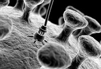
Of course, some things are just too small to be viewed by the microscope. Visible light is of a size of 300 - 800 nm, so it cannot resolve (or see) below this size. The answer was to use electrons instead of light, and the scanning electron microscope was born. This acts in a way not unlike the optical microscope, except instead of light waves, electron waves are used. This allows us to see down to about 10 nm. The next breakthrough was in 1986, when scanning probe microscopy was discovered by scientists at IBM. Using an instrument with a needle that had very fine tip, a couple of atoms wide, they were able not only to see atoms and molecules, but actually move them around. There is a very famous image of an IBM logo made of helium atoms on a solid surface. (The link is here) The scientists behind the development of this technique won a Nobel prize, their work opening up a new world to us, just as Hooke's microscope did in the 17th century. The reason these instruments can resolve down to nanometre level and below is that their tip is so fine, they can probe surfaces of a similar size.
Click here to read part 1.
Click here to read part 1.


Comments